Rick Dove, Paradigm Shift
International, www.parshift.com, ![]()
Oh yes . . . they also accommodate work flows of intermixed custom configured products -- the mass customization concept frequently misunderstood as the defining characteristic of Agile production. Mass customization is just one of many valuable change proficiencies possible in the Agile production operation.
The capabilities extolled above are not meant to be comprehensively defining, but rather to set the stage for a discussion about real machines and real production processes that do all of this. The example we use here is from the semiconductor manufacturing industry; but the principles and concepts illuminated are applicable in any industry.
The U.S. lost the semiconductor market to Japan in the ‘70s, and hopes for regaining leadership were hampered by a non-competitive process equipment industry - the builders of the "machine tools" for semiconductor fabrication. In this high paced industry, production technoligy advances significantly every three years or so, with each new generation of processing equipment cramming significantly more transistors into the same space.
With each new generation of equipment semiconductor manufacturers build a completely new plant, investing $250 million or more in equipment from various vendors, and twice that for environmentally conditioning the building to control micro-contaminates.
For equipment vendors, each new generation of process equipment presses the understandings of applied physics and chemistry. Million dollar machines are developed for depositing thinner layers of atoms, etching narrower channels, imprinting denser patterns, testing higher complexities, and sculpting materials at new accuracies and precessions. Generally each machine carries out its work in a reaction chamber under high vacuum, and sports a sizable supporting cast of controls, valves, pipes, plumbing, material handling, and whatnot.
New equipment development is actually new invention, frequently taking longer than the three-year prime-time of its life. And because the technology utilized in each generation is so unique, market success with one generation of equipment has little to do with the next or the last generation. The industry’s history is littered with small vendors that brought a single product-generation to market.
Single purpose, short lived, complex machines. Long equipment development cycles. Repeatability and reliability problems. All in a high volume, highly competitive production environment serving impatient, unforgiving markets. And every new generation requires a new plant with more stringent environmental conditioning to house the new machines. The learning curve in this industry is dominated by touchy equipment that takes half its product life to reveal its operating characteristics. Forget about rework here, and get used to scrap rates way above 50% in the early periods of production (You car builders may scoff at the low scrap cost, but this means lost deliverables with devastating loss of critical short-lived-market penetration). Equipment budgets routinely factor high outage expectations into extra machines -- million dollar machines -- and that’s the way it is in this industry.
Getting product out the door is so critical, and mastering the process so tough, that no one has time to question the craziness; or guts to say "I’m not going to take this anymore". Everybody is used to it. This is the way of semiconductors.
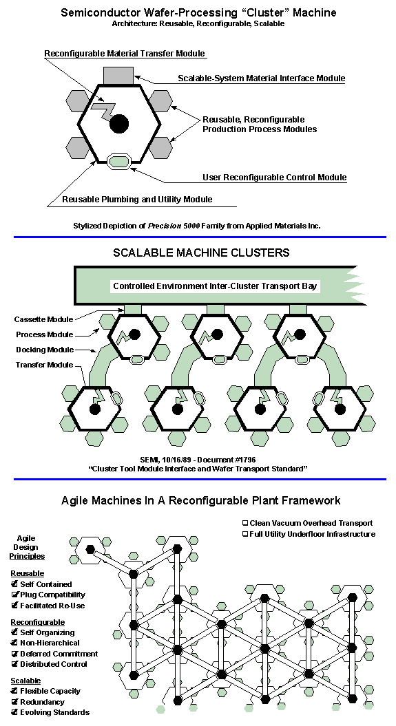
At least it was until something significant occurred in 1987: Applied Materials, Incorporated, a Sunnyvale, California-based company, brought a new machine architecture to market -- an architecture based on reusable, reconfigurable, scalable concepts.
The AMI Precision 5000 machines decoupled the plumbing and utility infrastructure from the vacuum chamber physics magic, and introduced the "multichamber" architectural concept. Instead of one dedicated processing chamber, these machines contained up to four independent processing modules serviced by a shared programmed
A single machine can integrate four sequential steps in semiconductor fabrication, decreasing the scrap caused by contamination during inter-machine material transfer. Yield rate is everything in the competitive race down the learning curve -- but this integrated modular approach pays other big dividends too.
Applied Materials shortened its equipment development time and cost significantly by separating the utility platform from the processing technology. Development resources are focused now on process technology, reusing the common utility base which accounts for 60% of the machine. This eliminates a significant design effort for each additional process capability Applied brings to market, and shrinks the complexity and time of shakeout and debug in prototyping stages. More importantly, perhaps, is the increased reliability that Applied’s customers enjoy with a mature and stable machine foundation.
In process sequences with disparate time differences among the steps, a configuration might double-up on two of the modules to optimize the work flow through a three-step process.
A malfunction in a process module is isolated to that module alone. It can be taken off-line and repaired while the remaining modules stay in service. The architecture also facilitates rapid and affordable swap-out and replacement servicing if repair time impacts production schedules.
Semiconductor manufacturing is barraged with prototype run requests from product engineering. New products typically require new process setups and often require new process capability. When needed, redundant process modules can be dedicated to prototyping for the period of test-analyze-adjust iterations it takes to get process parameters understand. And if a new capability is required, a single "outboard motor" is delivered quicker and at a lot less cost then a fully equipped and dedicated machine.
Cluster architecture also brings a very major savings in both time and cost for creating new fabrication facilities. The ultra-clean environment needed for work-in-process can be reduced to controlled hallways rather than the entire building. People can attend and service the machines without elaborate decontamination procedures and special body suits.
Work-in-process is most vulnerable to contamination when it is brought in and out of high vacuum. The cluster machine architecture reduces these occurrences by integrating multiple process steps in one machine. Using a docking module, these machines can be directly interconnected to increase the scale of integration.
Extending these concepts and combining them with a strategy for reconfigurable facilities might push the utility services below the floor and the clean transport above the machines. Though this "ultimate" configuration does not yet exist in a production environment, the possibility is obvious.
In 1989 the Modular Equipment Standards Committee of SEMI (Semiconductor Equipment and Materials International) started work on standards for mechanical, utility, and communications interfaces. What started as a proprietary idea at Applied Materials is moving toward an industry open architecture, promising compatible modular process units from a variety of venders.
Applied Materials revolutionized the semiconductor industry. Their cluster machines have propelled them into global leadership as the largest semiconductor equipment supplier in the world. Leadership is defined by followers, and today, every major equipment supplier in the world has a "cluster" tool strategy.
The Manufacturing Execution System (MES) software completes the total Agile production environment. This is the software that controls and schedules the routing of wafer batches through the production resources. Until recently these systems were no better at scheduling resources than your typical MRP that assumed infinite resources and had no clue about current plant status. In 1995 software vendors serving this market began introducing finite and real-time schedulers that reconfigure routings on the fly to optimize throughput.
Here we see the ten Agile system design principles that were introduced in last month’s column in action; with an Agile machine architecture that enables an Agile production environment. Next we will look at an equally Agile metal-cutting production operation; but with machine tools that are not themselves Agile.